Modem Bit Rate Timing
The modulator and the demodulator each have 4 possible sources for their bit rate timing.
The modulator always outputs the Send Timing signal, but the source of this timing may be either:
1. An internally generated bit rate NCO locked to the internal reference,
2. The Demodulator Receive Clock,
3. An external input at the data rate or
4. An external input on the Interface Terminal Timing input.
The modem’s internal reference is a 2.0 parts per million clock oscillator, which is sufficiently accurate for most applications. If system timing requirements dictate a better reference, the internal oscillator may be phase locked to an external reference applied at the rear panel.
The demodulator always outputs the Receive Timing signal. The Receive Demodulator Clock derived from the receive signal is synchronous with the Receive Data and is the normal source of the receive timing. If the system requires a different clock (which still must be the same average rate as the demodulator’s receive clock) then provisions are made to buffer the data in a programmable FIFO. The demodulator receive clock is always used to clock the data into the FIFO. The clock output can be either:
1. The Demodulator Receive Clock,
2. The Modulator Clock
3. An internally generated bit rate NCO locked to the Internal Reference, or
4. An external FIFO Clock applied on the interface connector.
If the demodulator receive clock is selected then the FIFO itself is physically bypassed by switching circuitry.
The internally generated bit rate NCO locked to the Internal Reference oscillator is settable to 40 bit accuracy. That is 1 part in 10 to the 12 or 1 part per trillion.
A block diagram simplified representation of the Transmit and Receive clock sources are shown
![]()
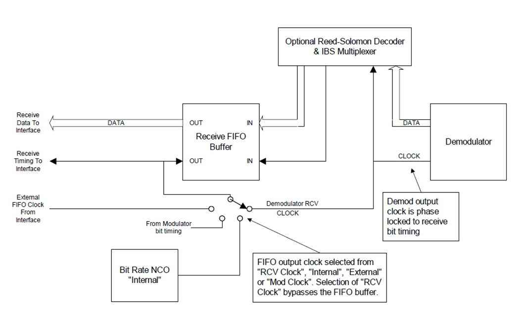
Receive Clock Sources
These Clock sources may be used in various ways in a system implementation to provide correct timing at a destination. Each of the clock sources can be set either from the front panel or from an external monitor and control system.